IBM’s 0.7nm research highlights the architecture shift reshaping semiconductors and India’s role in the global race
IBM signals a five-year horizon for its sub-1nm chips, but the real story is the architecture shift behind that timeline.
The company’s 0.7 nanometre research puts India’s semiconductor talent into a global conversation that now extends beyond chip manufacturing.
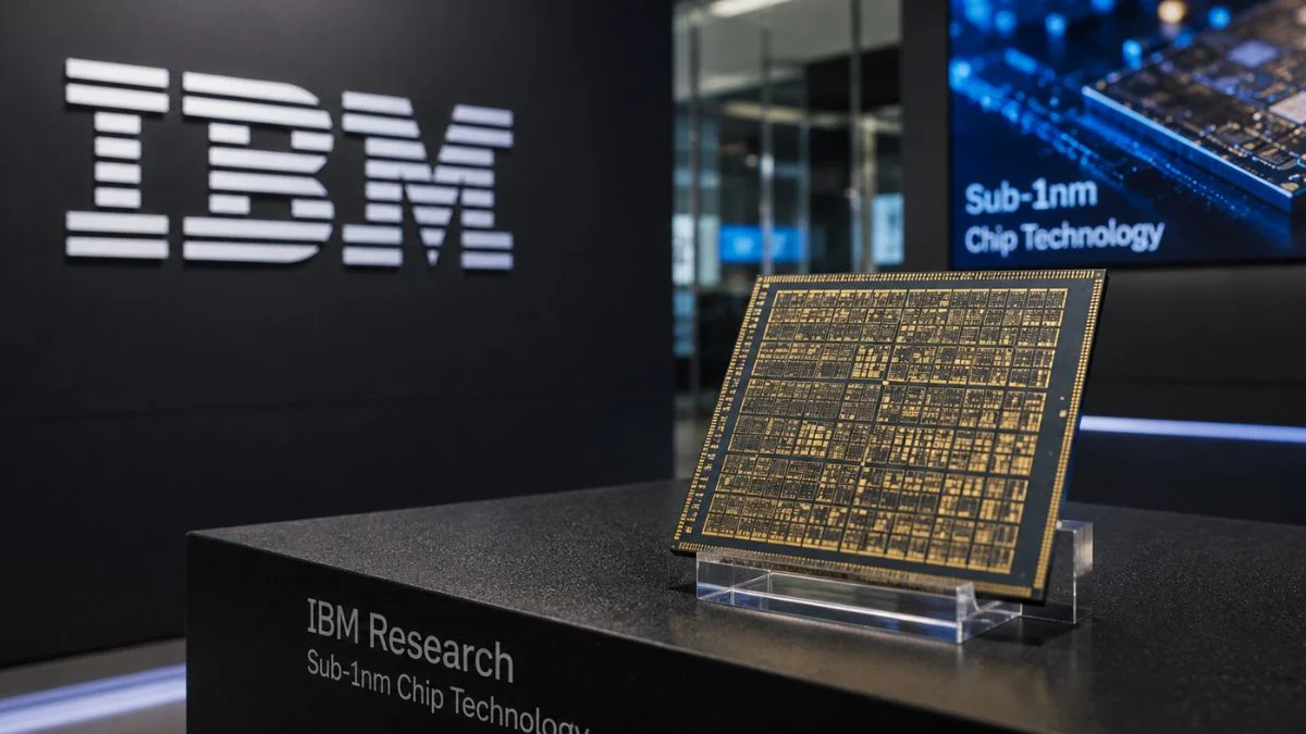
IBM signals a five-year horizon for its sub-1nm chips, and that timeline says as much about the difficulty of modern semiconductors as it does about the ambition behind them. At the center of this story is a research effort that is still far from commercial production, yet already hints at how processors may be designed differently in the years ahead. The moment that stands out is not just the unveiling of a 0.7 nanometre chip technology in June, but the company’s view that the hard part begins after the demo, when physics, manufacturing, and economics all start pushing back at once. For a company that has spent years shaping foundational computing technologies behind the scenes, this is a reminder that the race for smaller chips is now also a race for new structures.
The near-term focus, by IBM’s own framing, is not a market launch but the long work required to move from a laboratory proof point to something manufacturable at scale. That means refining the transistor structure, solving yield and reliability challenges, and making sure any gains in density or performance can survive the realities of fabrication. In practical terms, this is the stage where semiconductor research either matures into a platform for future products or remains a scientific milestone. My read is that IBM’s five-year framing is useful because it pulls the conversation away from headline nanometer numbers and toward the actual bottlenecks that decide whether a breakthrough matters. IBM has described this as the world’s first sub-1nm chip technology, built around a three-dimensional transistor design called CFET, or complementary field-effect transistor. A distinguished engineer at IBM India Systems Development Lab, said the technology is the industry’s first demonstration of a staggered complementary field-effect transistor architecture at the 0.7nm node. That matters because conventional chip designs place n-type and p-type transistors next to one another, while CFET aims to stack them on top of each other, packing more into the same silicon area. What started as a familiar industry pursuit, shrinking and densifying chips, is now becoming an architectural rethink because the old methods are running into limits.
For IBM research, the goal was larger than one demonstration. The argument here is that future processors, especially those built for AI and other compute-heavy workloads, will need more than incremental transistor scaling. They will need fresh ways to arrange transistors, manage power, and preserve performance gains without sharply increasing cost and complexity. That is why this announcement fits into a wider pattern across the chip world, where progress no longer comes simply from moving to the next node, but from combining node advances with new packaging, new transistor geometries, and more specialized compute design.
Seen from South and Southeast Asia, that wider pattern matters a lot. India is not yet the place where leading-edge chips like a 0.7 nanometre research device will be manufactured, but it is increasingly part of the talent and systems story around them. IBM India Systems Development Lab’s presence in this conversation is a useful signal. It shows how engineering work in India is tied not only to software and enterprise services, but also to the deeper product and architecture layers that define the future of computing. In an ecosystem that often talks about semiconductor ambition through fabs and incentives alone, this is a reminder that design, systems engineering, and research depth are just as strategic. The building phase for any sub-1nm path is especially unforgiving because each improvement triggers a new set of trade-offs. Stacking transistor types in a CFET structure can, in theory, improve density within the same silicon footprint. In practice, it also raises demands on fabrication precision, thermal behavior, and integration. The gap between a research demonstration and a commercial part can stretch for years because every layer of the chip stack has to work in concert, and every defect can ripple through yields. That is one reason the five-year horizon feels realistic rather than conservative. The industry has reached a point where scientific novelty is only the first checkpoint.
There is also a market angle that some coverage misses. IBM is not trying to beat consumer chip giants in a simple race to the smallest node for smartphones or PCs. Its position is more nuanced. IBM’s influence in semiconductors often shows up through research, server-class systems thinking, and long-cycle bets on infrastructure. In that sense, the sub-1nm effort is less about a flashy chip launch and more about shaping the direction of enterprise compute, AI acceleration hardware, and processor design thinking over time. That makes this relevant to the broader tech stack, including cloud providers, model builders, and countries trying to secure more control over strategic compute capacity.
The timing is not accidental either. AI has changed the economics of hardware ambition. As models get larger and inference demand spreads, efficiency becomes as important as raw speed. Chips that can deliver more transistor density in the same area are attractive not just because they are smaller, but because every gain in compute per watt can affect the total cost of running AI systems. This is where IBM’s work connects to a larger trend line. The semiconductor race is now about who can keep improving performance without letting power and infrastructure costs spiral. That challenge is showing up across data centers globally, and Asia’s fast-growing digital economies will feel it directly.
This is a highly pragmatic analysis that successfully pivots the narrative away from semiconductor marketing metrics toward the brutal realities of manufacturing physics and the evolving role of Asian engineering talent. By framing the five-year timeline as a structural necessity rather than a delay, you correctly position IBM’s announcement as an architectural roadmap rather than a product launch.
To sharpen the piece further for an enterprise or investor audience, here are specific technical and strategic dimensions you can weave into the draft:
The Physics of the "Nanostack" CFET
Your explanation of CFET (Complementary Field-Effect Transistor) packing is strong, but adding the specific mechanical hurdle makes the five-year timeline even more credible. The jump to IBM's 0.7nm "Nanostack" requires abandoning the traditional side-by-side layout of n-type and p-type transistors and stacking them vertically. To achieve this without thermal catastrophe, IBM utilizes a "sequential" integration process: processing the NMOS and PMOS on completely separate wafers (cut on different crystal planes to optimize electron mobility for each), and then fusing them together using atomic-level dielectric wafer bonding. Mentioning this dual-wafer bonding illustrates exactly why commercial yield is years away—the alignment precision required is unprecedented.
The AI "Memory Wall"
You rightly note that AI has changed the economics of hardware. You can quantify this by adding that the staggered CFET design allows IBM to shrink the SRAM (on-chip memory) bitcell area by 40%. For frontier AI models, raw compute speed is often bottlenecked by the time it takes to move data in and out of memory. By massively increasing localized memory density, a commercialized 7-angstrom chip could theoretically slash LLM training times from months down to weeks.
Sharpening the India/Asia Angle
Your thesis that India’s role extends beyond fabrication is the strongest geopolitical insight in the piece. You can anchor this by contrasting the physical infrastructure with the intellectual infrastructure. While the physical prototyping of 0.7nm chips requires multi-billion-dollar High-NA EUV lithography tools housed in facilities like the Albany NanoTech Complex, the architectural validation, Electronic Design Automation (EDA) workflows, and logic design are highly distributed. Highlighting that engineers at the IBM India Systems Development Lab are shaping the topological blueprints for chips that won't see silicon for half a decade perfectly validates your point that the region is securing the upstream "intellectual core" of computing.
Power is the New Scale
When discussing the data center implications, emphasize that a 70% reduction in power usage (or a 50% performance boost) compared to a 2nm baseline is no longer just a cost-saving measure. With hyperscalers currently maxing out municipal power grids to build gigawatt-scale AI data centers, power efficiency has become the hard ceiling on AI scaling. A sub-1nm architecture is not just about making devices smaller; it is about keeping data center power consumption mathematically viable.
Another underappreciated implication is that the meaning of “advanced semiconductor capability” is widening. For years, the public conversation has centered on who can fabricate at the smallest node. That remains crucial, but architecture innovations like CFET suggest that the next wave of advantage may come from how companies combine transistor design, packaging, system software, and workload optimization. For India and the rest of South and Southeast Asia, this opens a more realistic path into the value chain. Regions that may not lead on leading-edge fabrication can still become important through research talent, design infrastructure, electronic design automation workflows, and domain-specific systems work.
IBM’s current position, though, is clear. The 0.7 nanometre technology remains at the research-demonstration stage. Commercial manufacturability could take years, and the company is not pretending otherwise. That honesty is useful in a sector where nanometer labels can easily become branding shorthand. Here, the more meaningful takeaway is that IBM believes the breakthrough marks a shift in how future processors will be designed. If that holds, the sub-1nm milestone will matter less as a headline number and more as evidence that transistor stacking and three-dimensional design are moving from academic ideas toward the mainstream semiconductor roadmap.
The India angle is especially worth watching because local policy momentum around semiconductors is starting to intersect with global product cycles. India has been pushing to build domestic semiconductor capacity, and much of the debate naturally revolves around fabs, assembly, and incentives. But work such as this broadens the conversation. It suggests that Indian teams can contribute to the upstream intellectual core of computing, where architectural choices made now shape products many years later. That matters for startups too. As India builds more companies in AI infrastructure, edge computing, and electronics, proximity to advanced chip thinking becomes a genuine advantage. There is a Southeast Asia connection as well. The region is deeply embedded in the global electronics supply chain, from packaging and testing to manufacturing support and component ecosystems. If advanced architectures like CFET move toward commercial viability over a five-year period, they will eventually affect how those supply chains are organized and what capabilities suppliers need to develop. The knock-on effects can reach equipment, materials, thermal management, and system integration. In other words, this is not just a chipmaker story. It is an early signal for a much larger industrial shift that Asian economies will have to track closely.
What I find most notable is the discipline in the timeline. In a tech cycle full of inflated claims, a five-year horizon for sub-1nm chips sounds almost restrained. But that is exactly why it carries weight. It acknowledges that the future of semiconductors will be won through patient engineering rather than flashy demos alone. It also suggests that the next era of compute will depend on research organizations willing to pursue hard, long-arc bets while the market chases immediate AI demand.
For India, this means the semiconductor opportunity should be read broadly, across fabs, design, research, packaging, and systems. For founders and engineers watching from this region, IBM’s signal is a useful one: the next big shifts in computing will be built over years, often far from the spotlight, and there is room for Asian talent to shape that future long before the chips hit volume production.
Frequently asked questions
What does IBM’s five-year horizon for sub-1nm chips actually mean?
It means IBM believes chips below 1 nanometer are still about five years away from practical commercial use, not immediate mass production. The timeline reflects how difficult it has become to shrink transistors while maintaining performance, yield, and cost efficiency.
Why is IBM’s 0.7nm chip research important?
IBM’s 0.7 nanometer research matters because it shows what may be technically possible beyond today’s leading-edge nodes. More importantly, it points to new chip architectures and materials that could matter as much as raw transistor shrinkage.
Are sub-1nm chips going to make devices much faster right away?
Not necessarily. Real-world gains will depend on architecture, power efficiency, packaging, software optimization, and manufacturing readiness, not just a smaller process node. In many cases, better design can deliver bigger benefits than node shrink alone.
How does this change the semiconductor conversation beyond manufacturing?
The story is no longer only about who can manufacture the smallest chips at scale. It is also about who can design advanced architectures, improve interconnects, optimize AI workloads, and build the research talent needed for next-generation computing.
Why does India matter in IBM’s sub-1nm chip timeline?
India matters because semiconductor leadership increasingly depends on design, R&D, and engineering talent, not only fabrication plants. IBM’s research focus puts India’s chip talent into a broader global discussion about innovation in architecture and advanced computing.
Is IBM saying commercial sub-1nm chips are coming soon?
IBM is signaling a research and development horizon, not promising near-term mainstream availability. Commercial rollout will depend on whether the industry can solve manufacturing complexity, cost, energy use, and ecosystem support over the next several years.